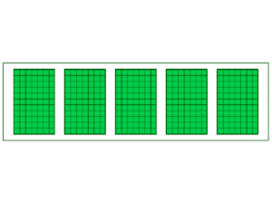
Optimizing Semiconductor and Photonics Substrate Layouts with MapSuite
Welcome to the forefront of semiconductor and photonics production, where MapSuite redefines substrate layout optimization for wafers, leadframes, trays, and final products. Explore the intricacies of substrate layout management with MapSuite, your all-in-one solution for enhancing efficiency and quality throughout the production process.
Understanding Semiconductor and Photonics Substrate Layouts
Semiconductor and photonics substrates, including wafers, leadframes, trays, and final products, play pivotal roles in the manufacturing of integrated circuits and optical components. Efficiently managing these layouts is critical for maximizing production yield, minimizing waste, and ensuring product quality.
Introducing MapSuite’s Substrate Layout Management
MapSuite offers a comprehensive suite of tools and features designed to streamline substrate layout management across all stages of production. From initial design to final inspection, MapSuite empowers engineers and manufacturers to optimize layouts and drive innovation in semiconductor and photonics manufacturing.
Join the MapSuite Revolution
Experience the power of substrate layout management with MapSuite. Enhance efficiency, drive innovation, and optimize production processes with MapSuite’s industry-leading tools and features. Whether you’re a semiconductor engineer, photonics manufacturer, or research institution, MapSuite empowers you to achieve excellence in substrate layout management.
Discover MapSuite today and revolutionize your approach to semiconductor and photonics production. Contact us to learn more about MapSuite’s capabilities and start maximizing your manufacturing potential.
Key Features of MapSuite for Substrate Layout Management
Wafer Mapping and Optimization: MapSuite enables engineers to visualize wafer layouts and optimize die placement for maximum yield and efficiency. From chip design to wafer fabrication, MapSuite’s wafer mapping tools ensure precise control over production processes.
Leadframe Design and Inspection: With MapSuite, leadframe design and inspection become seamless tasks. Visualize leadframe layouts, detect defects, and optimize material usage with MapSuite’s intuitive leadframe management tools.
Tray Layout Optimization: MapSuite’s tray layout optimization features empower manufacturers to maximize substrate utilization and minimize production waste. From component placement to tray organization, MapSuite provides the tools needed to optimize layout efficiency.
Final Product Inspection: MapSuite’s final product inspection capabilities enable manufacturers to ensure product quality and compliance with industry standards. From optical components to integrated circuits, MapSuite’s inspection tools provide insights that drive excellence in final product manufacturing.