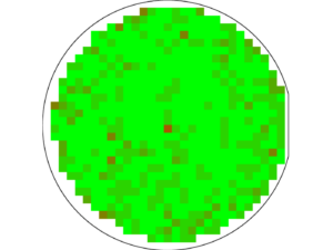
Elevate Your Analysis: Stacking Substrate Maps with MapSuite
Embark on a journey of advanced substrate analysis with MapSuite, where we redefine the process of stacking substrate maps for comprehensive batch and product analysis. From identifying defective areas on wafers to ensuring die position correctness and analyzing leadframe molding processes, MapSuite empowers you to unlock valuable insights and optimize production workflows.
Understanding Stacking Substrate Maps
In semiconductor and photonics manufacturing, the ability to stack substrate maps from a complete batch is essential for thorough analysis and optimization of production processes. Whether it’s identifying defective areas on wafers, ensuring correct die positions, or analyzing leadframe molding processes, efficient substrate map stacking is crucial for maximizing yield and product quality.
Introducing MapSuite’s Substrate Map Stacking Tools
MapSuite offers a comprehensive suite of tools and features designed to streamline substrate map stacking and enhance batch analysis capabilities. From defect identification to edge yield analysis, MapSuite empowers users to visualize, analyze, and optimize substrate maps with unparalleled precision and efficiency.
Join the MapSuite Revolution
Experience the power of substrate map stacking with MapSuite. Elevate your analysis, drive optimization, and achieve excellence in semiconductor and photonics production. Whether you’re analyzing wafers, leadframes, or other substrates, MapSuite empowers you to unlock valuable insights and maximize manufacturing potential.
Discover MapSuite today and revolutionize your approach to substrate map analysis. Contact us to learn more about MapSuite’s capabilities and start optimizing your production workflows for success.
Key Features of MapSuite for Substrate Map Stacking
Defective Area Analysis: MapSuite enables users to identify and highlight defective areas on wafers and leadframes within a complete batch. Visualize defect patterns, analyze defect distribution, and make informed decisions to improve production yield and quality.
Die Position Correctness: With MapSuite, users can ensure the correctness of die positions relative to substrate maps of a single batch. Detect misalignments, verify die placements, and optimize manufacturing processes to minimize errors and enhance overall yield.
Edge Yield Analysis: MapSuite’s edge yield analysis tools allow users to analyze edge defects and optimize edge yield in semiconductor and photonics production processes. Identify edge-related issues, implement corrective measures, and maximize substrate utilization for improved efficiency.
Molding Process Analysis: MapSuite provides insights into leadframe molding processes, enabling users to visualize and analyze molding defects, optimize mold designs, and enhance production efficiency. From material distribution to mold quality, MapSuite empowers users to drive innovation and excellence in leadframe manufacturing.